Overview
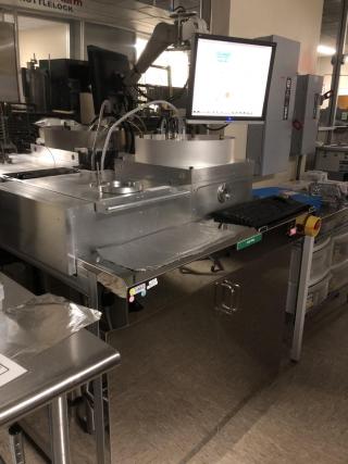
The Plasma-Therm Shuttlelock PECVD deposition, CCP-Dep, system is used primarily for depositing low-stress silicon nitride, silicon dioxide, amorphous and silicon carbide layers on 4 inch wafers. It can also be used for depositing silicon oxynitride layers, which have not been characterized at this writing. The stress level in the nitride films can be controlled by varying the He:N2
Processing Technique(s)
Capabilities and Specifications
Lab Supplied Materials
Material Thickness Range:
Process Temperature Range:
Substrate Type
Substrate Sizes
To maintain cleanliness level, cleans of both the chamber and wafers are required prior to processing -
Substrates in clean category: Pre-Diffusion Clean
For semi-clean substrates: Standard Metal Clean (SRS100 + PRS1000) . Run Chamber clean (no dummies) and conditioning with clean dummies prior to run
Lab Organization, Location, and NEMO Information
Training and Maintenance
Steps to become a tool user
Become a member of nano@stanford.
Become a member of SNF.
- Study the relevant operating procedures:
Shadowing is required. Contact a qualified lab member of the tool to arrange to ‘shadow’. It would be best to find someone who has used the system often. If you don’t know of anyone, you may check reservations or SNF usage to find a qualified user. We recommend that you be with the lab member for the full time while operating the tool and ask lots of questions during the shadowing. You may have to shadow a qualified user more than one time to be comfortable with the tool. Please follow the instructions on this form: Shadowing at SNF
- Contact the primary trainer: Lavendra Mandyam