Find here a collection "Nano Nuggets"- useful bits of information about different processing methods that should be helpful either in getting started or avoiding problems along the way. Some of them are parts of more detailed project reports, so if you want more info about a nugget, the report should be linked.
-
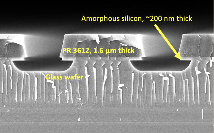
Resist Adhesion During Wet Etching
Tips for wet etching of glass substrates with resist adhesion problems.
-
Lesker2 Sputter TiN Initial Development
Our goal was to develop a process for sputtering of NVM-quality TiN using the new Lesker sputtering tool (Lesker-2) that resides inside the cleanroom. This tool can achieve the high-vacuum pressures necessary for TiN films with low levels of oxygen contamination.
-
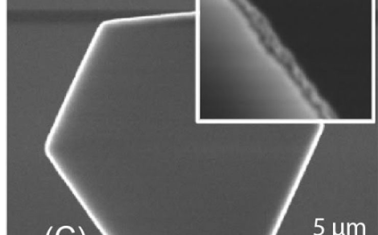
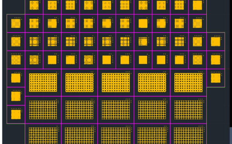
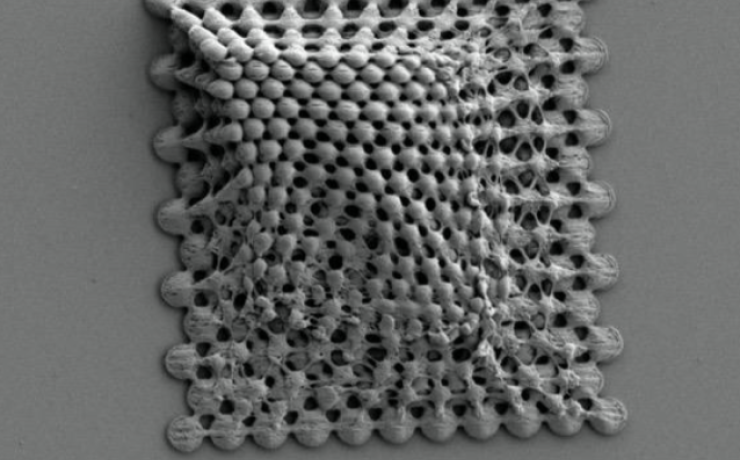
Self-Assembly Schemes for the Fabrication of Inverse Opals
The nanoscribe can be used to create template structures for particle self assembly, and details about inverse opal BCC and FCC structures are described.
-
SOP- Niobium structures releasing
We worked out a method for releasing niobium structures with high yield.
-
Post-metal etch clean
Procedures for troubleshooting post Nb-etch residues on Sapphire wafers are described.
-
SOP- Fabrication of an Etched Silicon Platform with Applications in Uniform Dissection of Biological Samples
This document contains standard operating procedures (SOPs) for the following processes: 1.Fabrication of oxide hard mask for deep silicon etching. 2.Tapered etch method for blade formation using PT-DSE 3.Through-hole etching using PT-DSE
-
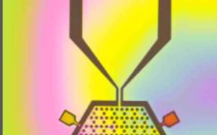
Improving adhesion and preventing collapsing of Nanoscribe resist IP-Dip
An improved substrate pretreatment protocol is therefore developed that results in better adhesion.
-
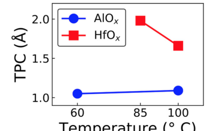
SOP for Thin, low temperature ALD of Al2O3 and HfO2 with seed layer
Tips for deposition of very thin, low temperature Al2O3 in the Savannah in the SNF.
-
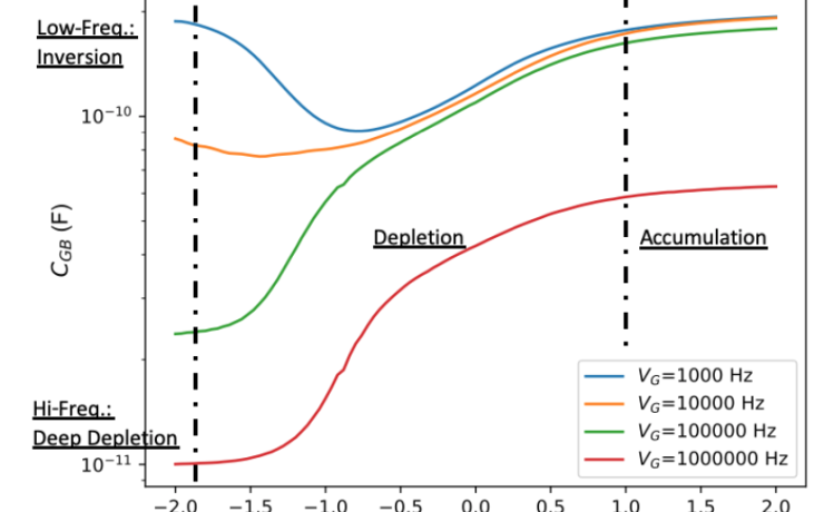
How to characterize thin ALD films
Both electrical and physical characterization techniques are explained for characterizing thin ALD films.
-
SOP for patterning Si wafers on heidelberg2
Some processing details for printing patterns for silicon nanowire fabrication.
-
SOP for Nano Imprint Lithography
Procedures for doing NIL in preparation for MACE etching.
-
SOP for Metal Assisted Chemical Etching (MACE)
Procedures for doing MACE etching to make tall pillars in silicon.
-
SOP for Seeded ALD deposition on MoS2
Standard operating procedures for seed layer aided ALD on 2D materials.
-
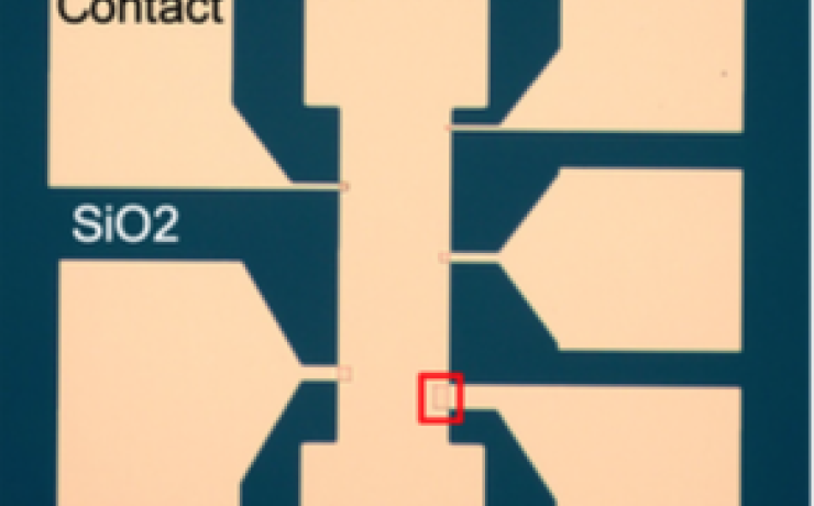
SOP for Seeded ALD depositions on MOSCAPS and MIMS structures on Silicon
Process to create electrical test structures using metal-seeded ALD layers on silicon substrates.
-
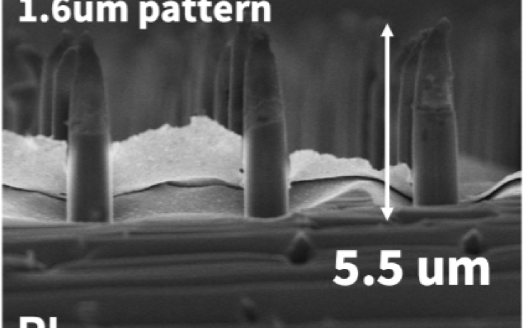
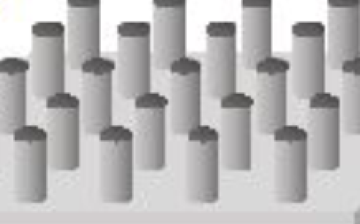
SOP for Making Vertical Nanostructures with Various Shapes
A two stage etching procedure can be used to fabricate various vertical nanostructures for bio-relatedexperiments.
-
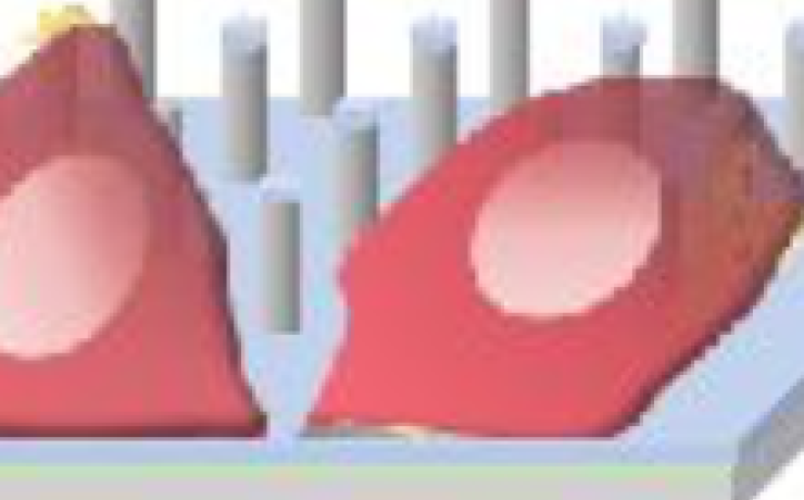
SOP for Bioprinting on Nanostructures
A guide to using a new PLPP gel protocol developed by Alveole.