Find here a collection "Nano Nuggets"- useful bits of information about different processing methods that should be helpful either in getting started or avoiding problems along the way. Some of them are parts of more detailed project reports, so if you want more info about a nugget, the report should be linked.
-
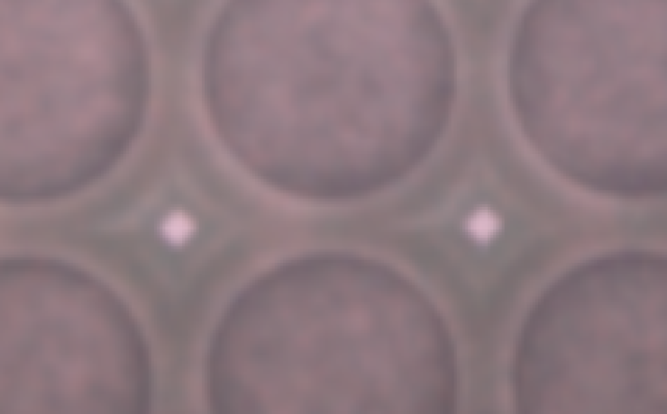
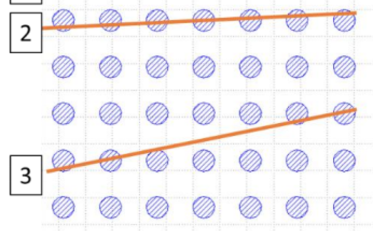
SOP for particle self assembly and RDF characterization
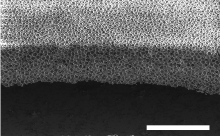
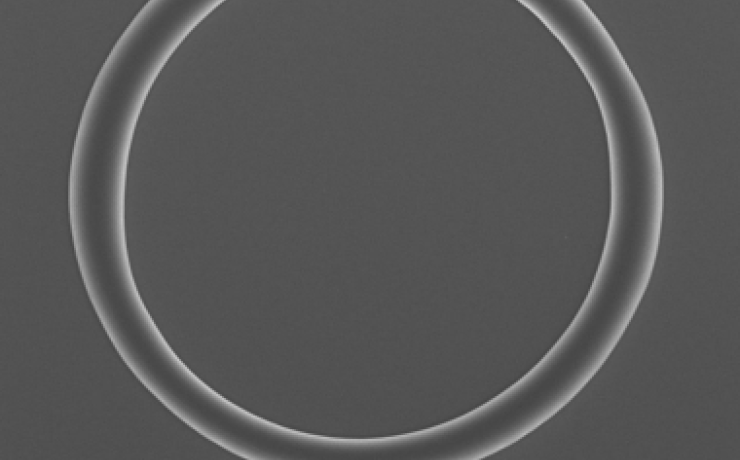
Highly monodisperse 4 um PMMA spherical particles were assembled in PDMS wells on either a silicon substrate or a glass coverslip. In order to quantify the order of one assembly compared to another, a radial distribution function (RDF) is used.
-
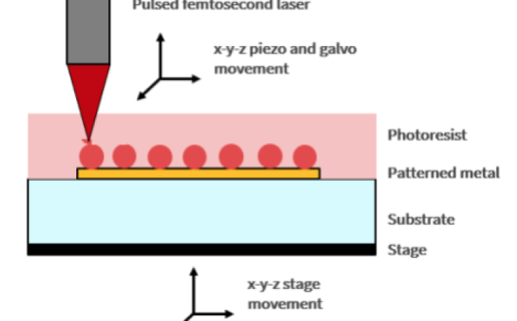
SOP for positive photoresist on Nanoscribe
SOP for using SPR-220 and AZ4620 positive photoresists on Nanoscribe using the oil immersion mode.
-
Patterning SPR220 on Reflective Materials with Nanoscribe
Processing details for using SPR-220 positive resist on a reflective metal surface to make 3D structures on the Nanoscribe.
-
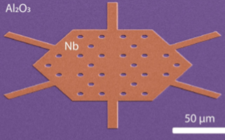
Niobium Deposition and Patterning Runsheet
Processing sequence for deposition and patterning of Niobium in the SNF.
-
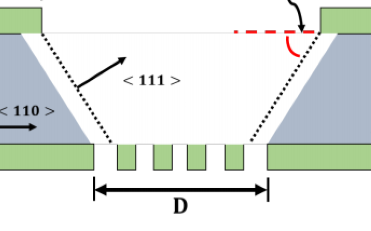
SOP- Silicon Oxide Hardmask for Si Etching in PT-DSE
Step-by-step procedures and processing tips for fabrication of an SiOx hardmask for deep silicon etch in the SNF.
-
Tips- Using Keyence for X-sectional Imaging
Tips for using the Keyence to image cross sections of wafer pieces. This can be used as a quick check before X-SEM.
-
Cross-sectional Characterization of Transferred DSA Holes using Focus Ion Beam
Here, we describe our strategy for inspecting the cross-section of features transferred from the BCP into an underlying hard material (e.g. SiO2, Si). -
Waveguide fabrication with the Heidelberg MLA150 Maskless Aligner Run Sheet
In order to make the lowest loss waveguides, we need to find a combination of dose/defocus and reflow time/temperature that gives us the best resolution and the lowest line edge roughness and line width roughness. -
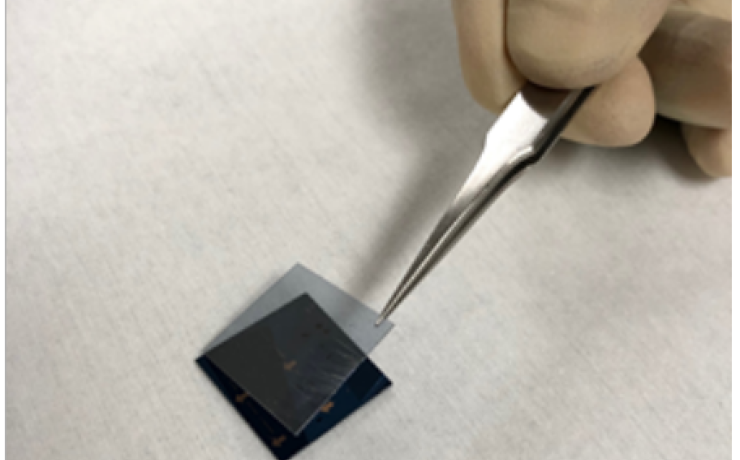
Characterization of TMDs and Contact schemes for Photovoltaic Applications- Standard Operating Procedure
The standard operating procedures for 1. Optimal TMD exfoliation on SiO2 substrate, 2. Etching of TMD flakes, 3. Transfer from TMD flakes from SiO2 substrate to a metallic substrate are explained in details. -
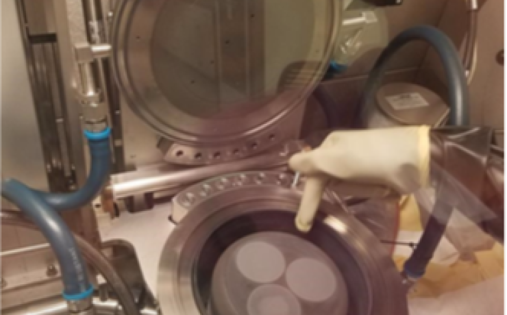
Standard Operating Procedure for MOCVD aix-ccs
This document describes things you need to check before operating the Stanford MOCVD aix-ccs tool for safety and correct operation.
-
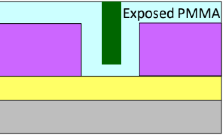
Block Copolymer Directed Self-Assembly Standard Operating Procedure
In this standard operating procedure (SOP), we propose a recipe for DSA with 70:30 PS-b-PMMA.
-
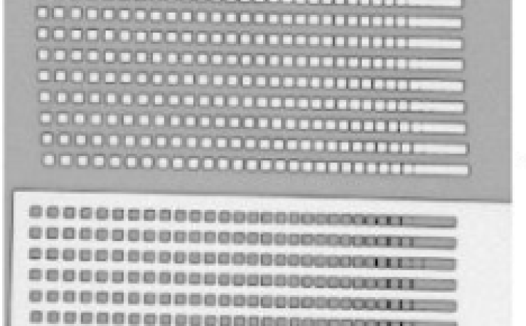
Silicon Nitride Nanoscale Stencils for Non-destructive Metal Grating Patterning
A process flow is presented to create periodic metallic gratings on the order of 150 nm using a stencil lithography technique.
-
Standard Operating Procedures for TMD exfoliation, etching, and transfer
The standard operating procedures for 1. Optimal TMD exfoliation on SiO2 substrate, 2. Etching of TMD flakes, 3. Transfer from TMD flakes from SiO2 substrate to a metallic substrate are explained in details.
-
Waveguide fabrication with the Heidelberg MLA150 Maskless Aligner
Process flow for optical waveguide creation using Heidelberg.
-
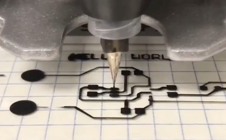
Voltera: Getting Started with Custom Inks
Watch E241 students load and print custom ink with the Voltera.
-
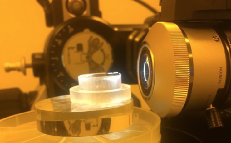
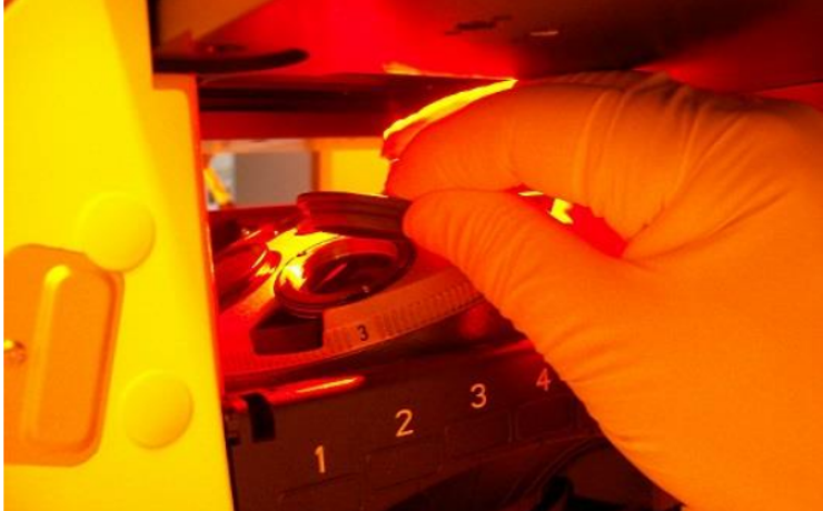
Stanford Nanoscribe Operating Procedure
This is the operating procedure written by our researchers for use of our Nanoscribe.